Semiconductor Interfaces at the Sub-Nanometer Scale -

-30% ar kodu BOOKS
Piegāde 22-28 darba dienu laikā
30 dienu atgriešanas politika
The Advanced Research Workshop on the Physical Properties of Semiconductor Interfaces at the Sub-Nanometer Scale was held from 31 August to 2 September, 1992, in Riva del Garda. Italy. The aim of the workshop was to bring together experts in different aspects of the study of semiconductor interfaces and in small-scale devices where the interface properties can be very significant It was our aim that this wo ... Pilns apraksts
Jums varētu patikt arī

Determined: The Science of Life Without Free Will
-30% ar kodu BOOKS
Piegādātāja noliktavā

The Light Eaters: How the Unseen World of Plant Intelligence Offers a New Understanding of Life on Earth
-30% ar kodu BOOKS
Piegādātāja noliktavā


Why We Sleep: Unlocking the Power of Sleep and Dreams
-30% ar kodu BOOKS
Noliktavā
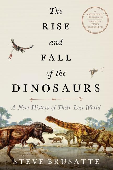
The Rise and Fall of the Dinosaurs: A New History of a Lost World
-30% ar kodu BOOKS
Piegādātāja noliktavā
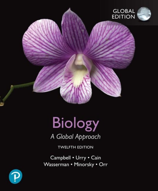
Biology: A Global Approach, Global Edition
Neil Campbell, Rebecca Orr, Lisa Urry, Peter Minorsky, Michael Cain, Jane Reece, Steven Wasserman
-30% ar kodu BOOKS
Piegādātāja noliktavā

Six Not-so-easy Pieces: Einstein's Relativity, Symmetry, and Space-Time
Richard P. Feynman, Robert B. Leighton, Matthew Sands
-30% ar kodu BOOKS
Piegādātāja noliktavā
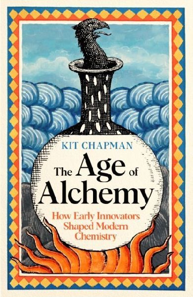
The Age of Alchemy: How Early Innovators Shaped Modern Chemistry
-30% ar kodu BOOKS
Piegādātāja noliktavā
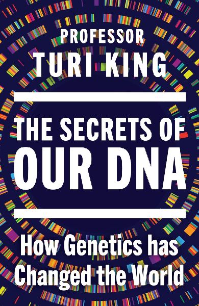
The Secrets of our DNA: How Genetics has Changed the World
-30% ar kodu BOOKS
Piegādātāja noliktavā

Janeway's Immunobiology
Leslie J. Berg, Kenneth Murphy, Casey Weaver
-30% ar kodu BOOKS
Piegādātāja noliktavā

How to Solve it: A New Aspect of Mathematical Method
-30% ar kodu BOOKS
Piegādātāja noliktavā

Factfulness: Ten Reasons We're Wrong About the World--and Why Things Are Better Than You Think
Ola Rosling, Anna Rosling Rönnlund, Hans Rosling
-30% ar kodu BOOKS
Piegādātāja noliktavā
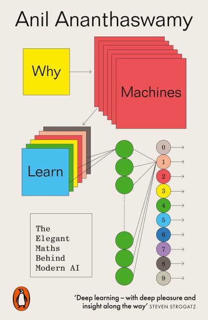
Why Machines Learn: The Elegant Maths Behind Modern AI
-30% ar kodu BOOKS
Piegādātāja noliktavā

The Feynman Lectures on Physics. The New Millennium Edition
Matthew Sands, Robert Leighton, Richard Feynman
-30% ar kodu BOOKS
Piegādātāja noliktavā
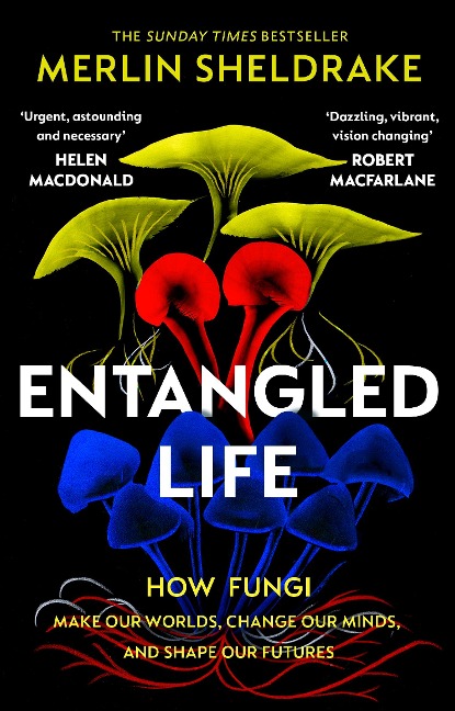
Entangled Life: How Fungi Make Our Worlds, Change Our Minds and Shape Our Futures
-30% ar kodu BOOKS
Piegādātāja noliktavā

Life As No One Knows It: The Physics of Life's Emergence
-30% ar kodu BOOKS
Piegādātāja noliktavā
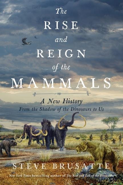
The Rise and Reign of the Mammals: A New History, from the Shadow of the Dinosaurs to Us
-30% ar kodu BOOKS
Piegādātāja noliktavā

Learn Faster, Perform Better: A Musician's Guide to the Neuroscience of Practicing
-30% ar kodu BOOKS
Piegādātāja noliktavā
The Brain That Changes Itself: Stories of Personal Triumph from the Frontiers of Brain Science
-30% ar kodu BOOKS
Piegādātāja noliktavā
Aprašymas
The Advanced Research Workshop on the Physical Properties of Semiconductor Interfaces at the Sub-Nanometer Scale was held from 31 August to 2 September, 1992, in Riva del Garda. Italy. The aim of the workshop was to bring together experts in different aspects of the study of semiconductor interfaces and in small-scale devices where the interface properties can be very significant It was our aim that this would help focus research of the growth and characterization of semiconductor interfaces at the atomic scale on the issues that will have the greatest impact on devices of the future. Some 30 participants from industrial and academic research institutes and from 11 countries contributed to the workshop with papers on their recent wode. . 'There was ample time for discussion after each talk. as well as a summary discussion at the end of the meeting. The major themes of the meeting are described below. The meeting included several talks relating to the different growth techniques used in heteroepitaxial growth of semiconductors. Horikoshi discussed the atomistic processes involved in MBE, MEE and MOCVD, presenting results of experimental RHEED and photoluminescence measurements; Foxon compared the merits of MBE, MOCVD, and eBE growth; Molder described RHEED studies of Si/Ge growth by GSMBE, and Pashley discussed the role of surface reconstructions in MBE growth as seen from STM studies on GaAs. On the theoretical side, Vvedensky described several different methods to model growth: molecular dynamics, Monte Carlo techniques, and analytic modeling.
Vairāk informācijas
| Izdevējs | Springer Netherlands |
|---|---|
| Series | NATO Science Series E: |
| Izlaides gads | 2012 |
| Vāka tips | Mīkstais vāks |
| EAN | 9789401049009 |